Perovskite passivation and 3D imaging of internal electrical behavior
A new scientific study published in the journal Newton introduces an advanced three-dimensional imaging technique to observe the internal electrical behavior of perovskite films used in solar cells, showing how perovskite passivation significantly improves efficiency.
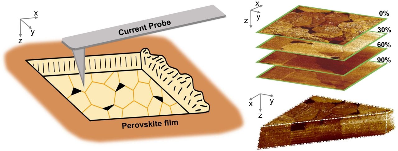
The research was carried out by scientists at the Ningbo Institute of Materials Technology and Engineering (NIMTE) of the Chinese Academy of Sciences and relies on conductive atomic force tomography microscopy. This approach reconstructs, with nanometer-scale resolution, the current distribution across the full thickness of the material.
The goal is to directly understand how different perovskite passivation treatments act on internal defects and how these defects influence charge transport, efficiency, and long-term stability. The results overcome the limits of traditional characterization techniques, which are often confined to surface measurements or averaged values, delivering a complete three-dimensional view of the film’s electrical structure and linking microscopic features to the final performance of photovoltaic devices.
Why internal defects reduce perovskite solar cell performance
Perovskite solar cells are made from polycrystalline films, where rapid crystallization promotes the formation of structural defects. The study shows that, without passivation, these imperfections translate into low-conductivity regions that can occupy a significant share of the active volume.
Three-dimensional maps reveal that in non-passivated samples, high-resistance regions account for more than 15% of the film at mid-thickness, extending more than 400 nanometers deep.
These areas disrupt continuous charge pathways, slow carrier diffusion, and increase non-radiative recombination losses. The result is a drop in open-circuit voltage and fill factor, two parameters that are critical to overall solar cell efficiency.
The three-dimensional analysis also highlights that defect distribution is far more complex than surface-only measurements suggest, confirming that the electrical quality of perovskite films depends on the entire volume, not just the top interface.
How bulk perovskite passivation reshapes charge transport
Bulk perovskite passivation acts directly during film formation by introducing chemical additives into the precursor solution. Tomographic images show that this strategy sharply reduces high-resistance regions already within the interior of the material.
At a depth corresponding to 50% of the film thickness, the fraction of resistive areas drops to around 1.3%, compared with much higher values in untreated samples. At the same time, conductivity along grain boundaries rises markedly, with increases ranging from +152% to +265% compared with the grain interiors.
These findings indicate that bulk perovskite passivation does more than neutralize point defects. It improves the continuity of vertical charge-transport channels throughout the film. The resulting current uniformity reduces local fluctuations and enables more efficient carrier diffusion, laying the groundwork for higher overall electrical performance in perovskite solar cells.
Surface perovskite passivation and its impact on interfaces
Surface perovskite passivation primarily affects regions near the top interface of the device. Measurements initially show reduced surface conductivity due to the presence of the passivation layer, but after removing just a few nanometers, the current increases noticeably.
High-resistance regions decrease rapidly with depth and are nearly absent beyond 50% of the film thickness. This behavior suggests that surface perovskite passivation does not remain confined to the surface but penetrates along grain boundaries, helping to reduce defects in underlying regions as well.
From a device perspective, this effect is especially important because it improves the interface with charge-transport layers, lowers recombination losses, and supports higher open-circuit voltage.
Combined perovskite passivation delivers peak efficiency and stability
The most significant results emerge when bulk and surface perovskite passivation are combined. In this case, three-dimensional maps reveal a highly conductive internal structure, with residual resistive regions almost entirely confined to the surface.
Devices fabricated with this combined strategy reach a power conversion efficiency of 25.1%, compared with 23.3% for non-passivated cells. Stability also improves markedly. After 400 hours under ambient conditions, cells with combined perovskite passivation retain 86% of their initial efficiency, versus 55% for untreated devices.
Electrical data further show a sharp reduction in surface recombination velocity, from 660 to 230 cm/s, along with a significant drop in trap density, down to 5.7 × 10¹⁵ cm⁻³. Together, these results directly link the three-dimensional electrical quality of perovskite films to both performance gains and long-term durability in next-generation solar cells.